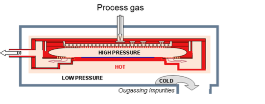
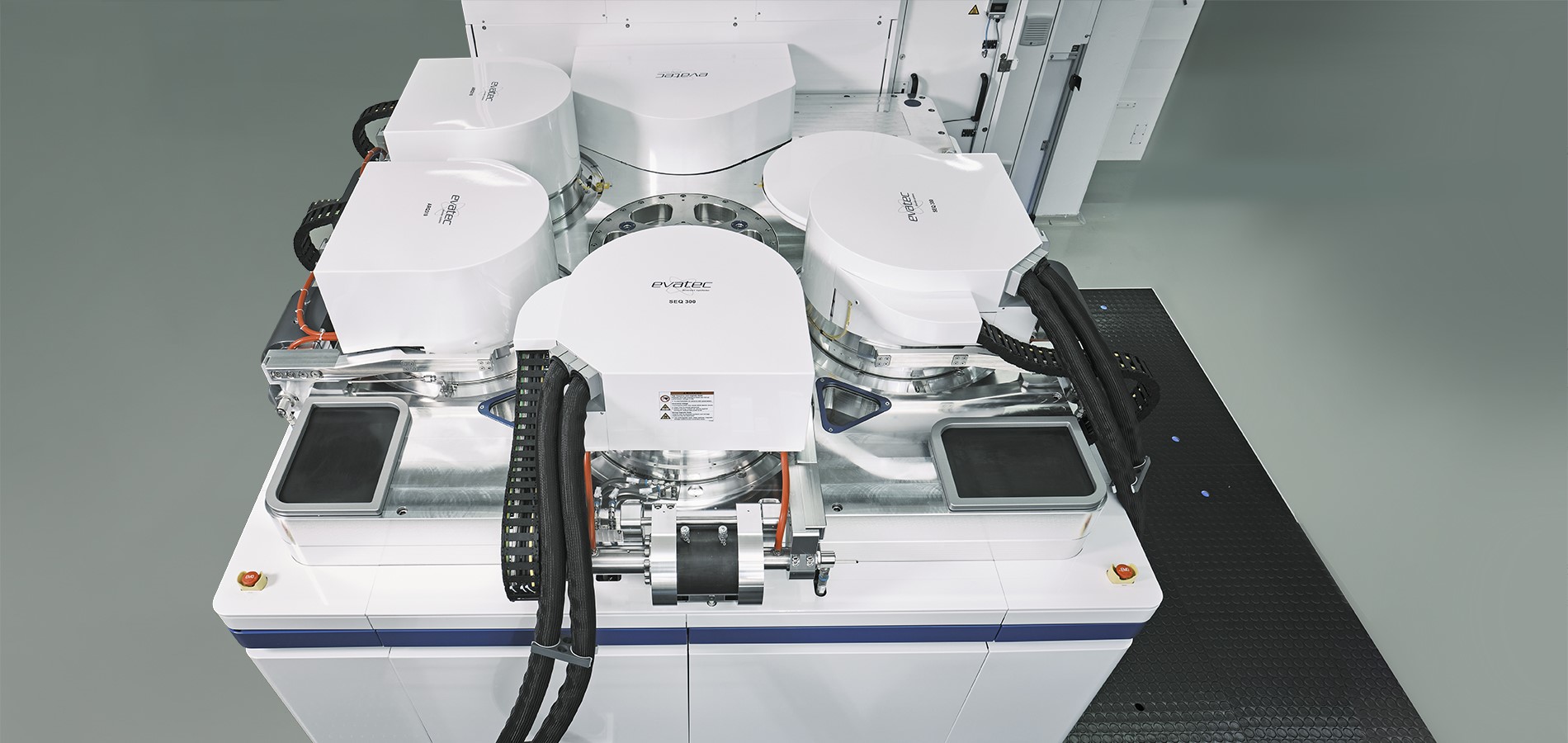
Plasma box
Choose Plasmabox for pinhole free, high purity films and simple reactor maintenance
Test Modal

Ullenda voluptaspe natem. Ceped quam rem. Nemped que porehen ihilitatis quas endest etur alis as id quatium expelic imoluptatur repe dendere ribus, sam nonserferum nessit que vel maxim re porro od quam dolo dusaectore aperuptae qui volore, comnisquo tem incto blacepu digniet pra dit labo. Tis aspid et everfer ovidestis derro tem sedis eicabo. Optaspe rferia volesenes erro quam, sitatus solut quiatum res same atem hitiam vento is videbit velit deror autatem.
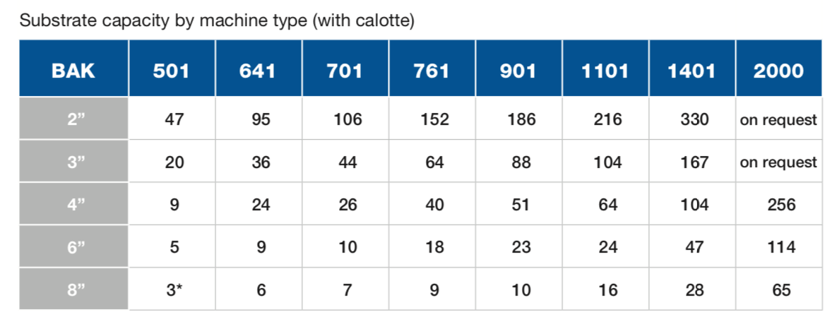
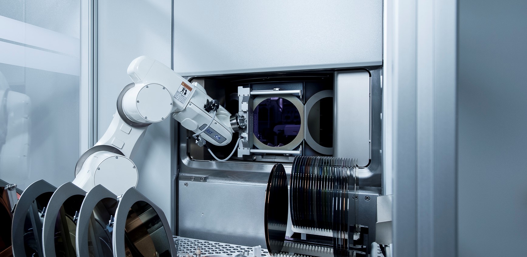
From the smallest to the biggest- get an idea how many substrates our systems can hold in a single batch
Test Modal
Ullenda voluptaspe natem. Ceped quam rem. Nemped que porehen ihilitatis quas endest etur alis as id quatium expelic imoluptatur repe dendere ribus, sam nonserferum nessit que vel maxim re porro od quam dolo dusaectore aperuptae qui volore, comnisquo tem incto blacepu digniet pra dit labo. Tis aspid et everfer ovidestis derro tem sedis eicabo. Optaspe rferia volesenes erro quam, sitatus solut quiatum res same atem hitiam vento is videbit velit deror autatem.

Company Overview
About us
Company Overview
Thin Film technology shaping the lives of millions around the globe
For 80 years, thin film technology has been at the center of global innovation. With its origins from the Balzers AG corporation in 1946, Evatec today enables the production of advanced semiconductors, optoelectronic and photonic applications. Thin films produced on Evatec systems enable new levels of performance in communication networks, smart devices, electric and autonomous vehicles, healthcare systems and industrial electronics.
Driven by the demand for ever smaller and more energy efficient devices, thin film deposition plays a decisive role in enabling progress in sensing, imaging, connectivity and energy management. Evatec’s expertise ensures that next‑generation devices can operate with higher precision, improved speed, greater reliability and energy efficiency — from the development of next generation 6G mobile network to micro LED technology delivering mass market augmented reality wearables , and high performance computing for Artificial Intelligence.
What we make
From R&D to high‑volume manufacturing, Evatec delivers thin film production tools and processes to customers around the globe. With already 80 years of process know‑how, we enable robust thin film production processes for current and future device technologies. Our platforms combine etch and deposition technologies using advanced process control methods to ensure production at high yields and the best cost of ownership.
Explore our full range of systems and contact your local sales and service organization or visit the individual product pages.
BAK FAMILY
Flexible family of evaporators in sizes from 0.5 to 1.4 meters for R&D or mass production.
CLUSTERLINE® FAMILY
Flexible family of fully automated cluster tools up to 650mm for single substrate processing.
HEXAGON
Dedicated platform for wafer level advanced packaging applications like FOWLP.
LLS EVO
Vertical batch sputter platform with a proven track record in the semiconductor industry.
SOLARIS® FAMILY
Family of high speed inline sputter platforms for high volume production in fully automated fabs.
Our Technology
Thin film technologies that give you the lead
Evatec delivers complete thin film production solutions combining advanced deposition platforms equipped with Evatec proprietary source technologies, and decades of thin film engineering experience. We support customers across Advanced Packaging, Semiconductor, Optoelectronics and Photonics markets, applying our core competences in etch, evaporation, sputter, PECVD and PEALD.
Advanced Process Control on Evatec platforms increases throughput, yield and process stability. Plasma emission monitoring controls stoichiometry and enhanced deposition rates for higher throughputs in reactive processes, whilst quartz and optical systems ensure precise layer thickness and process repeatability.
Evaporation Technology
Evatec’s evaporation expertise originates from the Balzers electron‑beam platforms and has been refined over decades. Supreme source stability combined with optimized materials usage and advanced In situ control technologies deliver precise, highly repeatable thin films, in optical, optoelectronic and semiconductor applications.
Sputter Technology
Our sputter tools use Evatec’s proprietry cathode technologies tailored for diverse material and device requirements. In all cases long target lifetimes and stable deposition conditions ensure reproducible results and excellent cost of ownership.
Plasma Etch Solutions
ICP and CCP plasma sources support surface modification, cleaning and controlled layer removal. These processes improve adhesion, interface quality and overall stability in downstream deposition steps.
PECVD with PLASMABOX
PLASMABOX source technology provides low temperature PECVD with high purity and uniformity on CLUSTERLINE® tools. It supports deposition of dielectric layers for semiconductor, optoelectronic and photonic applications under sensitive thermal budgets and with in situ source cleaning reducing maintenance efforts within the fab.
PEALD Technology
Evatec’s PEALD module enables the deposition of high‑purity dielectric layers with excellent conformality and precise thickness control on planar and structured substrates. Integrated into the CLUSTERLINE® 200 platform, it allows low‑temperature processing and seamless combination with etch, PVD and PECVD steps without breaking vacuum. This supports uniform, damage‑free layers for applications in semiconductor, MEMS, RF and Power Device manufacturing.

Evatec Competence Laboratory (ECL)
The Evatec ECL offers ISO4‑capable facilities equipped with more than 30 deposition tools and over 20 measurement methods. Together with customers and research institutions it supports collaborative development of new processes, materials and layer stacks and bridges early‑stage R&D with industrial manufacturing.
Click here to read more about the setup of this facility in 2019.
Our Markets
Leveraging know-how across complimentary markets
Evatec supports a wide range of applications built on 80 years of thin film expertise. Our core markets include: Frontend, Wafer Level Packaging, Panel Level Packaging, Power Devices, Wireless, MEMS, Discrete LED / Laser, Wafer Level Optics, Precision Optics, Functional Coatings.
Technology Transfer Across Markets
In a world of rapid change where "semiconductor" is converging with "optics", Evatec makes use of its 80 years of know-how, transferring experience in one market to support developments in another. On one hand, the optical monitoring control capabilities first developed by Evatec for traditional optical film applications are now helping our customers in selected optoelectronic and semiconductor applications to achieve new levels of performance for their next generation devices. On the other hand, the fully automated wafer handling methods developed for production platforms in the semiconductor industry are now supporting our customers in emerging wafer level optics applications for optical quality layers at high yields and particle free processing.
Markets Driven by IOT and Digitalization
Evatec know-how enables the expanding IoT landscape, where sensing, communication and processing require precision, miniaturization and speed at high energy efficiencies. Evatec's thin film expertise helps customers accelerate technology roadmaps and adopt reliable thin film production solutions for emerging device generations.
Advanced Process Control & Engineering Excellence
Evatec advanced process control solutions integrate know-how in multi-domain engineering, plasma physics, and vacuum technology into “in situ” measurement and real time tuning of thin film production processes that provide:
- Precision and repeatability for best process yields
- Higher throughputs for volume production at the lowest cost of ownership
- Scalable performance in development of new materials and device types
With more than 200 patents, Evatec continues to advance thin film deposition for semiconductor, optoelectronic and photonic applications.

Did you know?
In 2025 we published our first Sustainability Report.
Please take a moment to explore and learn more about where we started and where we're heading.
People, Knowledge & Global Support Network
Evatec’s global organization includes highly skilled engineers and specialists who support customers in development or 24/7 high volume manufacturing. With locations in Europe, Asia and the United States, we provide training to our customers and back up service that ensures stable, reliable equipment operation and long equipment lifetimes by installing new capabilities and technologies through retrofits as our customer’s needs evolve.
To read our corporate social responsibility policy click here.
Commitment to Quality, Sustainability & Responsible Manufacturing
At Evatec we follow ISO 9001 and ISO 14001 standards, emphasizing structured quality management, resource efficiency and sustainable product design. Our environmental efforts include waste reduction, lower emissions, energy efficiency improvements and responsible end‑of‑life considerations.
To view our ISO certification in English or German you can click the following links ISO 9001 English , ISO 9001 German , ISO14001 English , ISO14001 German
Vision for the Future
Evatec’s long‑term vision is to enable innovations in energy efficiency, connectivity, mobility, data processing and smart sensing through advanced thin film technologies. As AI, autonomous mobility and advanced healthcare accelerate, precise thin film deposition becomes increasingly essential. Evatec supports these trends by delivering systems that enable higher device performance, lower power consumption and enhanced functionality.
To read more about our vision, mission and environmental policy click here
Want to know more?
To read more about Evatec production platforms, process technologies and markets please go to the individual pages of our web site or read the case studies in our LAYERS magazines.